
Views: 0 Author: Site Editor Publish Time: 2026-08-17 Origin: Site


High-power density electronics, advanced optoelectronics, and semiconductor manufacturing face a critical physical limit. They must dissipate extreme heat while maintaining strict electrical isolation. Traditional substrates like Alumina fail to meet the thermal conductivity requirements of next-generation components. This limitation creates severe thermal bottlenecks, reduces component lifespans, and ultimately causes system failures. Conversely, high-performance alternatives like Beryllium Oxide introduce severe toxicity risks, triggering complex regulatory compliance hurdles and inflating handling requirements.
Aluminum Nitride Ceramic has emerged as the baseline standard for solving this exact engineering conflict. It bridges the gap between thermal dissipation and electrical insulation. This guide evaluates the material properties, comparative trade-offs, and implementation realities of specifying this material for high-stakes thermal management applications. You will learn how to match substrate capabilities directly to your engineering requirements.
Exceptional Thermal-Electrical Balance: AlN delivers a thermal conductivity of 170–230 W/m·K (nearly 5x to 7x that of Alumina) while maintaining high dielectric strength and electrical insulation.
Silicon Compatibility: Its Coefficient of Thermal Expansion (CTE) closely matches that of Silicon (Si) and Gallium Arsenide (GaAs), preventing mechanical stress and delamination in semiconductor assemblies under thermal cycling.
Regulatory Compliance: AlN provides a non-toxic, RoHS-compliant alternative to Beryllium Oxide without sacrificing high-end thermal performance.
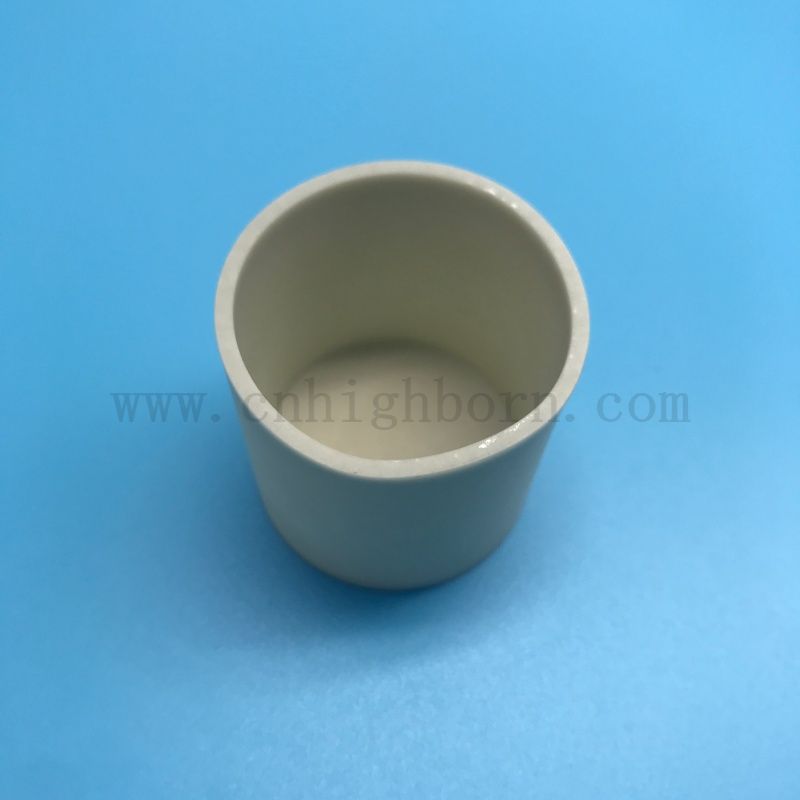
Application Specificity: While highly effective for heat sinks, substrates, and high thermal conductivity AlN crucible applications, its higher cost, moisture sensitivity, and machining complexity require precise qualification against project requirements.
Modern electronics continue to shift toward extreme miniaturization. Devices now output significantly higher power within much smaller footprints. Insulated-Gate Bipolar Transistor (IGBT) modules, high-brightness LEDs, and 5G RF modules generate massive thermal loads. Heat accumulates rapidly at the semiconductor junction. If you fail to extract this heat efficiently, the junction temperature exceeds safe operational limits. This leads directly to thermal runaway and immediate device failure. Engineers must design thermal pathways that move heat from the die to the ambient environment with minimal resistance.
Standard metallic heat sinks made of copper or aluminum offer excellent thermal conductivity. However, they are highly electrically conductive. Many high-power applications require strict electrical isolation between the semiconductor die and the cooling infrastructure. You cannot mount a high-voltage component directly to a copper block without causing a short circuit. Inserting polymer-based thermal interface materials provides insulation but creates a massive thermal barrier. This exact problem necessitates the use of advanced ceramic substrates that act as both heat conductors and electrical insulators.
Thermomechanical stability presents another major engineering hurdle. Semiconductors heat up and cool down rapidly during operation. Substrates and semiconductor dies expand at different rates when exposed to these temperature changes. This mismatch in the Coefficient of Thermal Expansion (CTE) induces severe mechanical stress. Over time, thermal cycling causes solder joint fatigue. It leads to micro-cracking, delamination, and premature device failure. You must select materials that expand at similar rates to prevent this mechanical degradation.
Evaluating a thermal substrate requires strict adherence to specific success metrics. You must measure the following parameters to determine if a material fits your application:
Thermal conductivity (W/m·K) to determine raw heat transfer efficiency.
Dielectric strength (kV/mm) to establish the electrical isolation capacity and prevent arcing.
Coefficient of Thermal Expansion (ppm/°C) to verify mechanical compatibility with silicon dies.
Dielectric constant (Dk) to ensure signal integrity in high-frequency RF applications.
Commercial aluminum nitride typically delivers a thermal conductivity range of 170 W/m·K to 230 W/m·K. This performance relies entirely on the mechanism of phonon scattering. In non-metallic solids, heat does not travel via free electrons. Instead, it travels via phonons, which are quantized modes of vibrations in the crystal lattice. Any defect in this lattice scatters the phonons and degrades thermal transfer. Therefore, the absolute purity of the ceramic directly dictates its thermal performance.
Oxygen impurities present the greatest threat to thermal conductivity. Oxygen atoms substitute for nitrogen in the crystal lattice, creating vacancies that scatter phonons aggressively. Manufacturers use specific sintering aids to solve this problem. Yttria (Y2O3) is commonly added during the manufacturing process. The yttria acts as a getter, reacting with oxygen impurities to form yttrium aluminate phases. These phases migrate to the grain boundaries during high-temperature sintering, leaving the primary crystal lattice highly purified and structurally sound.
This purification process results in exceptional thermal transfer efficiency. When compared to standard FR4 printed circuit boards, aluminum nitride offers nearly two orders of magnitude better heat dissipation. It also vastly outperforms standard oxide ceramics, making it the premier choice for dense power electronics where every degree of temperature reduction extends the operational lifespan of the semiconductor.
Thermal conductivity means little in power electronics without corresponding electrical isolation. Aluminum nitride excels here, offering a volume resistivity greater than 10^14 Ω·cm. Its dielectric strength typically ranges from 15 to 20 kV/mm. This robust insulation allows engineers to mount high-voltage components directly onto the substrate without risking electrical breakdown or partial discharge events.
Direct mounting eliminates the need for secondary insulating layers. Polymer films or thermal pads inherently impede heat transfer. By removing them, you drastically lower the overall thermal resistance of the assembly. The heat moves directly from the die, through the ceramic, and into the cooling mechanism. This direct path is critical for managing the transient thermal spikes common in motor drives and power inverters.
The material also demonstrates exceptional stability in RF and microwave applications. It features a dielectric constant of approximately 8.8 at 1 MHz. Combined with a very low dielectric loss tangent, it prevents signal degradation at high frequencies. This makes the substrate highly stable for advanced telecommunications, radar systems, and 5G infrastructure components where signal integrity is just as critical as thermal management.
Mechanical reliability depends heavily on CTE matching. Aluminum nitride features a CTE of approximately 4.5 ppm/°C at room temperature. This value aligns remarkably well with standard semiconductor materials. Silicon exhibits a CTE between 2.6 and 3.2 ppm/°C, while Gallium Arsenide is similarly matched. Copper, by comparison, expands at roughly 17 ppm/°C, creating massive strain if bonded directly to silicon.
This close alignment produces a specific operational outcome. When the semiconductor assembly undergoes rapid thermal cycling, the die and the substrate expand and contract at nearly the same rate. This minimizes the shear stress applied to the solder joints and bonding layers. Without this matching, the continuous expansion and contraction would quickly shear the solder, creating voids that block heat transfer and cause immediate thermal runaway.
Reducing thermomechanical stress directly increases device reliability. Applications operating in harsh environments demand this stability. Aerospace components, military electronics, and automotive EV inverters rely on this precise CTE matching to survive thousands of extreme temperature cycles without mechanical failure. It ensures the physical integrity of the package matches its electrical performance.
Despite its robust physical properties, aluminum nitride possesses a specific chemical vulnerability. It is susceptible to hydrolysis. When exposed to high-humidity environments or liquid water, the material reacts with moisture. This reaction forms aluminum hydroxide and releases ammonia gas. Over time, hydrolysis degrades the structural integrity and thermal performance of the substrate, turning the surface into a chalky, non-conductive layer.
Engineers must implement strict mitigation strategies to prevent this degradation. You cannot deploy raw aluminum nitride in non-vacuum or high-humidity environments without protection. Manufacturers apply specific passivation layers or glass coatings to seal the ceramic surface. These coatings block moisture ingress while maintaining the underlying thermal properties of the substrate.
In highly demanding applications, hermetic sealing provides the ultimate protection. By enclosing the substrate within a sealed, moisture-free package, you completely eliminate the risk of hydrolysis. Understanding this environmental limitation ensures long-term reliability in field deployments, preventing unexpected failures in humid operating conditions.
Material Comparison Chart
| Material | Thermal Conductivity (W/m·K) | CTE (ppm/°C) | Dielectric Strength (kV/mm) | Primary Advantage |
|---|---|---|---|---|
| Aluminum Nitride (AlN) | 170 - 230 | ~4.5 | 15 - 20 | High thermal transfer with CTE matching |
| Alumina (Al2O3) | 25 - 30 | ~7.2 | 15 | Low cost, easy metallization |
| Beryllium Oxide (BeO) | ~250 | ~8.0 | >20 | Highest thermal conductivity (Legacy) |
| Silicon Nitride (Si3N4) | 60 - 90 | ~3.2 | 15 | Extreme mechanical strength |
Alumina remains the most common ceramic substrate in the electronics industry. However, its thermal performance is limited. Alumina delivers a thermal conductivity of roughly 25 to 30 W/m·K. In contrast, an AlN thermal management ceramic provides 170+ W/m·K, moving heat exponentially faster away from critical junctions. This massive difference dictates component density limits.
Alumina offers distinct practical advantages. It is significantly cheaper to produce. It is easier to metallize using standard industry processes because it is an oxide ceramic. Furthermore, it is completely immune to moisture degradation, requiring no specialized passivation layers or hermetic sealing for environmental protection.
You must apply a strict decision rule here. Specify aluminum nitride only when thermal loads explicitly exceed Alumina's dissipation capacity. It is also justified when strict space constraints prevent the use of larger, bulkier Alumina heat sinks. For low-power applications with ample physical space, Alumina remains the practical and economical choice.
Historically, Beryllium Oxide dominated high-end thermal management. BeO offers slightly higher thermal conductivity, peaking around 250 W/m·K. It also features a lower dielectric constant, which benefits certain high-frequency RF applications where signal propagation speed is the absolute priority.
The critical failure point of BeO lies in its severe toxicity. Inhaling BeO dust causes berylliosis, a chronic and often fatal lung disease. This toxicity triggers massive OSHA and RoHS compliance costs. Facilities require specialized handling protocols, dedicated machining environments, and expensive disposal liabilities that complicate the entire manufacturing pipeline.
The modern engineering decision rule is absolute. Aluminum nitride serves as the mandatory replacement for BeO in all new designs. Environmental Health and Safety (EHS) mandates dictate this shift globally. The minor performance trade-offs in thermal conductivity are entirely offset by the elimination of toxicity risks and the simplification of the supply chain.
Silicon Nitride occupies a specific niche in power electronics. While aluminum nitride offers superior thermal conductivity, Si3N4 excels in physical durability. Silicon Nitride provides vastly superior mechanical strength, fracture toughness, and bending strength, making it highly resistant to physical impacts.
This distinction dictates their respective use cases. Recommend Si3N4 for environments subjected to extreme mechanical shock or heavy vibration. Specific EV drivetrains and heavy industrial machinery often utilize Si3N4 substrates to prevent the ceramic from shattering under physical stress.
Conversely, specify aluminum nitride for applications where maximum heat dissipation represents the primary bottleneck. If the environment is mechanically stable but thermally extreme, AlN remains the superior choice. You trade mechanical toughness for raw thermal extraction capability.
The semiconductor industry relies heavily on advanced ceramic substrates. Insulated-Gate Bipolar Transistor (IGBT) modules manage massive power loads in rail traction, industrial drives, and renewable energy inverters. These modules generate intense heat that must be dissipated instantly to prevent failure. The substrate acts as the primary thermal bridge between the silicon and the liquid cooling plate.
Power MOSFETs and high-frequency RF/microwave packages for 5G infrastructure face similar challenges. The dense packaging of these components leaves no room for bulky cooling systems. Aluminum nitride substrates pull heat directly away from the silicon dies, allowing engineers to pack more processing power into smaller enclosures without violating thermal limits.
By maintaining lower junction temperatures, these substrates prevent thermal runaway. They ensure stable electrical performance across high-density power grids and continuous-duty telecommunications infrastructure. The material provides the foundational thermal stability required to keep modern power networks operational under peak loads.
Thermal management extends beyond electronic substrates into advanced materials processing. A high thermal conductivity AlN crucible plays a vital role in specialized manufacturing. These crucibles are utilized extensively in crystal growth processes, specifically for pulling Gallium Arsenide (GaAs) and Silicon Carbide (SiC) boules where precise thermal gradients are mandatory.
They also support OLED manufacturing and high-temperature metallurgical processes. The material demonstrates exceptional resistance to molten metals, including highly reactive aluminum and lithium. It does not contaminate the melt, ensuring high-purity output for sensitive semiconductor-grade materials.
Furthermore, these crucibles maintain structural stability in inert or reducing atmospheres at extreme temperatures. They can operate effectively at temperatures approaching 2000°C. This stability provides the uniform heat distribution critical for defect-free crystal growth, preventing thermal shock from shattering the crucible during rapid cooling phases.
High-power UV LEDs and industrial laser diodes generate significant heat within a microscopic footprint. If this heat remains trapped, the diode suffers immediate performance degradation. Aluminum nitride submounts provide the necessary thermal extraction path, pulling heat away from the active light-emitting region.
Efficient heat extraction directly correlates to device stability. In laser diodes, temperature fluctuations alter the emission wavelength. By stabilizing the temperature, the ceramic submount ensures strict wavelength stability. This is critical for fiber optic communications and precision laser cutting tools where wavelength drift causes system failure.
For high-brightness LEDs, thermal management maintains luminous efficacy. Heat degrades the phosphor layers and reduces light output over time. Proper heat dissipation maximizes the operational lifespan of the diode, ensuring consistent performance over thousands of hours of continuous operation.
Working with fully sintered aluminum nitride presents significant manufacturing challenges. The material exhibits extreme hardness and inherent brittleness. Standard machining tools will fail immediately. Post-sintering modifications require specialized equipment and strict operational protocols to prevent micro-cracking.
Engineers must follow a strict sequence for manufacturing and quality assurance:
Green-State Forming: Shape the raw ceramic powder using pressing or tape casting before it hardens.
Green Machining: Drill vias and cut complex geometries while the material is still soft to minimize tool wear.
High-Temperature Sintering: Fire the ceramic in a nitrogen atmosphere with yttria additives to achieve full density.
Diamond Grinding: Use specialized diamond-grit wheels to achieve final surface flatness and tight dimensional tolerances.
Laser Ablation: Utilize precision lasers for micro-vias or fine-feature cutting that grinding cannot achieve.
Thermal Verification: Test batch samples using the Laser Flash Method (ASTM E1461) to guarantee thermal conductivity specifications.
Engineers must practice strict Design for Manufacturability (DFM). You should design components to minimize post-fire machining. Whenever possible, utilize green-state machining. Shaping the ceramic before it undergoes high-temperature sintering drastically controls production costs and reduces material waste.
Integrating the ceramic into an electronic assembly requires metallization. Because aluminum nitride is a non-oxide ceramic, it is inherently difficult to metallize compared to Alumina. The surface lacks the oxygen atoms that traditional bonding metals typically grip. You cannot simply print copper onto the raw surface and expect it to adhere under thermal stress.
Manufacturers utilize specific metallization techniques to overcome this. Direct Bonded Copper (DBC) requires intentionally oxidizing the AlN surface to create a thin alumina layer, allowing the copper to bond at high temperatures. Active Metal Brazing (AMB) skips the oxidation step by using a braze alloy containing active metals like titanium, which chemically reacts directly with the nitride surface. AMB generally provides superior reliability for extreme thermal cycling.
Direct metallization optimizes thermal resistance. It eliminates the need for thick, highly resistive Thermal Interface Materials (TIMs) between the ceramic and the copper traces. However, you must monitor quality closely. If the metallization profiles are not strictly controlled by the manufacturer, you risk severe adhesion failure, leading to delamination during field operation.
Aluminum nitride ceramic stands as the definitive material of choice when standard ceramics fail thermally and metallic heat sinks fail electrically. It bridges the critical gap in modern power electronics, offering unmatched thermal conductivity alongside robust dielectric strength. Its physical properties align perfectly with the demands of next-generation semiconductor packaging.
Engineers should specify this material when designing high-power density systems like IGBTs, industrial lasers, and 5G RF modules. When CTE matching with Silicon, non-toxic high thermal conductivity, and strict electrical isolation are non-negotiable, this ceramic provides the exact engineering solution required.
Map your exact thermal load requirements against Alumina limitations to justify the material upgrade.
Specify your metallization requirements based on specific bonding needs, choosing carefully between DBC and AMB processes.
Consult with technical ceramics manufacturers during the initial design phase to optimize for green-state machining tolerances.
Define strict environmental passivation strategies if deploying the substrate in non-vacuum or high-humidity applications.
A: In an oxygen-rich environment, aluminum nitride begins to oxidize at approximately 700°C, forming an alumina layer that degrades thermal performance. However, in inert or reducing atmospheres, the material remains highly stable and can operate effectively at temperatures exceeding 1900°C.
A: The manufacturing process is significantly more complex. It requires the precise synthesis of high-purity AlN powder, the addition of specific yttria sintering aids, and high-temperature processing in controlled nitrogen atmospheres. These stringent manufacturing requirements drive up production costs.
A: Yes. The material is susceptible to hydrolysis. It reacts with liquid water or high ambient moisture to form aluminum hydroxide and ammonia gas. Commercial applications prevent this degradation by applying passivation layers, glass coatings, or utilizing hermetic sealing.
A: Yes. It exhibits extremely low outgassing properties, making it highly suitable for Ultra-High Vacuum (UHV) applications. It is frequently used in semiconductor wafer processing equipment and vacuum-sealed electronic packages without contaminating the environment.
A: Its Coefficient of Thermal Expansion (~4.5 ppm/°C) closely matches that of Silicon dies. This alignment ensures both materials expand and contract at similar rates during thermal cycling. This minimizes shear stress, preventing solder joint fatigue and micro-cracking.
A: It replaces BeO functionally to eliminate toxicity risks, but it is not a perfect drop-in replacement. AlN has a slightly different dielectric constant and requires different metallization processes. Engineers must make minor design adjustments to accommodate these differences.
A: The most common compatible techniques include Direct Bonded Copper (DBC), Active Metal Brazing (AMB), and thin-film sputtering. These specialized processes are necessary because AlN is a non-oxide ceramic, requiring specific bonding mechanics to ensure strong metal adhesion.