
Views: 0 Author: Site Editor Publish Time: 2026-08-16 Origin: Site


High-power electronics and wide-bandgap semiconductors require packaging solutions that can manage extreme thermal loads and high currents without mechanical failure. Specifying the wrong ceramic base for a direct bonded copper application leads to premature thermal fatigue, substrate delamination, or unnecessary overspending on over-engineered materials. Evaluating the exact thermal, mechanical, and chemical properties of available ceramics—primarily Aluminum Oxide and Aluminum Nitride—is critical for engineering teams to balance performance requirements with manufacturing viability. We need to look at how these materials behave under stress on the test bench and in the field. You must match the substrate to the specific thermal output of your semiconductor die. Getting this right prevents catastrophic module failure during aggressive power cycling. The baseline requirements for power modules demand high dielectric strength, high thermal conductivity, and robust current-carrying capacity.
Material Dichotomy: Aluminum Oxide (Al₂O₃) remains the cost-effective standard for general power electronics, while Aluminum Nitride (AlN) is mandatory for high-power density applications requiring superior heat dissipation.
Manufacturing Realities: Non-oxide ceramics like AlN require a precise pre-oxidation step to form the eutectic bond with copper, adding complexity to the DBC process.
Thermo-Mechanical Balance: Substrate selection must prioritize Coefficient of Thermal Expansion (CTE) matching with the semiconductor die to prevent solder joint fatigue during thermal cycling.
Defining the baseline requirements for power modules involves looking at high dielectric strength and high thermal conductivity. You also need robust current-carrying capacity. A reliable Metallized Ceramic Substrate provides the foundation for these performance metrics. It acts as the critical interface between the heat-generating semiconductor die and the cooling system. When you mount a silicon carbide MOSFET, the heat flux density is massive. The substrate must pull that heat away instantly while maintaining strict electrical isolation up to several kilovolts.
The direct bonded copper process bonds high-purity copper directly to a ceramic base. We typically use Oxygen-Free High-Conductivity (OFHC) copper. This utilizes a high-temperature copper-oxygen eutectic melting process at approximately 1065°C. The furnace atmosphere is tightly controlled with trace amounts of oxygen. This method eliminates the need for intermediate adhesive layers. Adhesives typically impede heat transfer and degrade under extreme temperatures. The resulting bond is both mechanically robust and thermally efficient. The eutectic liquid wets the ceramic surface, and upon cooling, forms a permanent chemical and mechanical bond.
Pre-bonding processing and quality control dictate the success of the final module. Raw ceramic bases undergo precise laser cutting, scribing, and rigorous cleaning. We cannot tolerate any organic residues or particulate contamination on the ceramic surface. Critical surface roughness and flatness inspections are required. We look for a specific Ra value to ensure the copper can grip the ceramic. These checks guarantee uniform eutectic wetting and prevent interfacial micro-voids during bonding. A void at the interface acts as a thermal insulator, creating a hotspot that will eventually destroy the semiconductor die.
A direct bonded copper ceramic consistently outperforms traditional printed circuit boards and insulated metal substrates. It handles high-voltage and high-temperature environments with ease. FR4 boards simply burn up under these loads. Insulated metal substrates suffer from the high thermal resistance of their dielectric polymer layers. The thick copper layers on a DBC carry massive currents, while the ceramic provides essential electrical isolation without sacrificing thermal conductivity. This makes it the only viable choice for traction inverters, grid-tied solar inverters, and heavy industrial motor drives.
We also have to consider the layout and etching process. After the copper is bonded, we apply a photoresist, expose the circuit pattern, and etch away the unwanted copper. The etching chemistry must be aggressive enough to remove thick copper but controlled enough to prevent severe undercutting of the traces. Undercutting reduces the cross-sectional area of the trace, which increases electrical resistance and generates unwanted heat. We monitor the etch factor closely on the production line to maintain trace integrity.
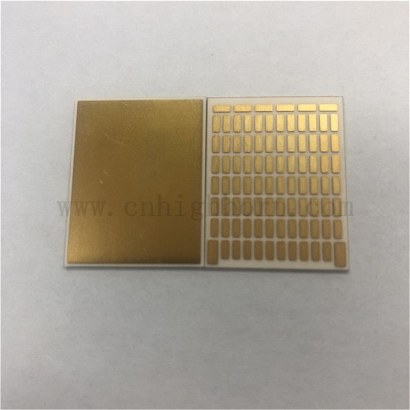
Aluminum Oxide offers a thermal conductivity of 24 to 30 W/mK. It provides excellent mechanical stability and high dielectric strength. We typically use 96% purity Al₂O₃ for standard DBC applications. The remaining 4% consists of sintering aids like silica and magnesia, which help densify the ceramic during firing. This material naturally bonds with copper during the DBC process due to its existing oxide state. It requires no chemical pre-alteration. You just clean it and run it through the bonding furnace.
You will find Al₂O₃ in standard industrial motor drives, consumer power electronics, and low-to-medium power IGBT modules. It is highly reliable for applications where the thermal flux is manageable. The mechanical strength is sufficient for standard vibration profiles found in factory environments. When designing with Al₂O₃, we usually limit the copper thickness to 0.3mm to prevent the higher CTE of the copper from cracking the ceramic during thermal cycling. It is a proven, stable material that forms the backbone of the power electronics industry.
Aluminum Nitride delivers exceptional thermal conductivity, ranging from 170 to 230 W/mK. Its CTE closely matches silicon and silicon carbide chips. This close CTE match drastically reduces the shear stress on the solder joint between the die and the substrate during power cycling. As a non-oxide ceramic, AlN must undergo a controlled pre-oxidation process. We bake the bare AlN substrates in an oxidizing atmosphere at high temperatures. This creates a critical micro-thin surface layer of Al₂O₃ before the copper can successfully bond.
If the oxidation layer is too thin, the copper won't bond. If it is too thick, the thermal resistance increases, defeating the purpose of using AlN. An AlN DBC circuit substrate is ideal for EV traction inverters, high-power RF modules, and aerospace power systems. These applications demand maximum heat extraction in the smallest possible footprint. The material is brittle, so handling during assembly requires specialized tooling to prevent edge chipping.
Zirconia Toughened Alumina offers higher fracture toughness than standard Al₂O₃. We add zirconium oxide particles to the alumina matrix. When a crack tries to propagate through the material, the zirconia particles undergo a phase transformation that expands their volume, effectively pinching the crack shut. It proves highly useful for environments experiencing extreme mechanical vibration, such as downhole drilling equipment or heavy off-highway vehicles.
Silicon Nitride provides the highest mechanical strength and thermal cycling reliability. It has a very high fracture toughness and a moderate thermal conductivity around 90 W/mK. However, manufacturers typically pair Si₃N₄ with Active Metal Brazing rather than standard DBC due to complex bonding requirements. The AMB process uses a brazing paste containing active metals like titanium to chemically react with the silicon nitride. This creates an incredibly strong bond that can withstand thousands of severe thermal shocks without delaminating.
Evaluating the trade-off between heat dissipation and mechanical strength is a primary engineering task. AlN favors rapid heat transfer, whereas ZTA and Si₃N₄ excel in fracture toughness. You must calculate the thermal resistance across the entire substrate stack to ensure operational stability. We use finite element analysis to model the heat flow from the semiconductor junction, through the solder, into the copper trace, across the ceramic, and down into the baseplate.
| Material | Thermal Conductivity (W/mK) | CTE (ppm/K) | Bending Strength (MPa) | Primary Application |
|---|---|---|---|---|
| Al₂O₃ (96%) | 24 - 30 | 6.8 - 8.2 | 300 - 400 | Standard IGBTs, general power modules |
| AlN | 170 - 230 | 4.5 - 4.7 | 300 - 450 | High-density SiC/GaN, EV inverters |
| ZTA | 24 - 28 | 6.8 - 7.5 | 400 - 600 | High-vibration industrial modules |
| Si₃N₄ | 80 - 90 | 2.5 - 3.2 | 600 - 800 | Extreme reliability automotive (AMB) |
DBC configurations standardly utilize two layers of copper. This symmetrical top and bottom cladding balances tensile stress during cooling. Layout symmetry rules prevent substrate warpage, commonly known as the bimetallic strip effect. If you have a large solid copper pad on the bottom and heavily etched thin traces on the top, the substrate will bow like a potato chip when it cools down from the 1065°C bonding temperature. Maintaining this balance is crucial for reliable module assembly. We often add dummy copper pads on the top side purely to balance the mechanical stress.
The ceramic's CTE interacts directly with the copper layers and the semiconductor die. Managing mismatch stresses at the joint interface prevents premature failure. Standard copper thicknesses range from 0.127mm to 0.3mm. Design rules dictate trace spacing, isolation gaps, and edge pull-back to prevent arcing and mechanical stress concentrations. We pull the copper back from the edge of the ceramic by at least 0.5mm. This prevents electrical arcing across the edge and stops micro-cracks from initiating at the ceramic boundary where stress is highest.
Current capacity is directly tied to copper thickness and trace width. We calculate the required cross-sectional area based on the maximum continuous current and the allowable temperature rise. For a 200A module, you might need 0.3mm thick copper with very wide traces. You also have to design for surge currents, which can be ten times the continuous rating for a few milliseconds. The thermal mass of the thick copper helps absorb these transient energy spikes before they can overheat the ceramic.
Mismatched thermal expansion between thick copper layers and the ceramic base causes stress during aggressive power cycling. The copper wants to expand much faster than the ceramic. This leads to delamination at the edges of the copper traces. Mitigate this by implementing dimpled copper designs or stepping copper edges. A stepped edge reduces the stress concentration at the interface. Transitioning to AMB serves as a solution for extreme reliability requirements, as the brazed joint is far more ductile than the eutectic bond.
We test for this using severe thermal shock chambers. We cycle the substrates from -40°C to +150°C for thousands of cycles. We then inspect them using Scanning Acoustic Microscopy. SAM uses high-frequency sound waves to detect microscopic air gaps between the copper and the ceramic. If we see delamination starting at the corners of the traces, we know the design needs adjustment. Sometimes simply rounding the corners of the copper pads in the layout can significantly increase the cycle life.
Inconsistent oxidation layers on AlN lead to weak eutectic bonds and localized hot spots. If the furnace atmosphere fluctuates during the pre-oxidation bake, the oxide layer will be uneven. This compromises module integrity. Specify strict quality control metrics for peel strength. We solder a wire to a copper pad and pull it at a 90-degree angle until it breaks. We measure the force required in Newtons per millimeter. Use ultrasonic scanning to detect microscopic voids before assembly.
We also perform cross-sectional analysis using a Scanning Electron Microscope. We cut the substrate, polish the edge, and look at the bond line under high magnification. We want to see a continuous, uniform transition from copper to copper oxide to aluminum oxide to aluminum nitride. Any gaps or brittle intermetallic phases indicate a process failure. Controlling the oxidation furnace profile is the most closely guarded secret of top-tier AlN substrate manufacturers.
AlN powder and manufacturing processes are significantly more expensive and have longer lead times than Al₂O₃. The raw powder requires high purity and specialized handling to prevent moisture absorption. Utilize Al₂O₃ for prototyping and low-power variants. Reserve AlN strictly for high-power density applications where thermal budgets dictate its necessity. Do not specify AlN just for a safety margin if the thermal calculations show Al₂O₃ will keep the junction temperature within limits.
Work closely with your procurement team to forecast AlN demand accurately. The lead times for high-quality AlN substrates can stretch to several months during industry shortages. Qualify multiple suppliers early in the design phase. Ensure that both suppliers can meet your specific peel strength and voiding specifications. A dual-source strategy protects your production line from unexpected disruptions in the raw material supply chain.
Selecting the right manufacturing partner ensures long-term reliability. You need a supplier who understands the metallurgy and the ceramics. Use this checklist to evaluate potential suppliers before signing a production contract:
Request traceability reports on ceramic powder purity, specifically verifying 96% versus 99.6% Al₂O₃.
Verify copper oxygen content documentation to ensure optimal eutectic bonding.
Check for peel strength standards and minimum N/mm requirements. We look for at least 50 N/cm.
Review thermal shock cycling limits and partial discharge characteristics.
Assess supplier competency in fine-line etching and surface finishes like Ni/Au, Ag, or OSP.
Confirm the use of ultrasonic non-destructive testing for void inspection on every production batch.
Audit their pre-oxidation process controls if you are purchasing AlN substrates.
Examine their dimensional tolerance capabilities for laser cutting and hole drilling.
The choice of ceramic material dictates the thermal ceiling and mechanical lifespan of the power module. Al₂O₃ remains the pragmatic choice for standard applications. AlN is non-negotiable for high-density, wide-bandgap semiconductor packaging. Base your decision on a strict calculation of required thermal resistance, expected thermal cycling profiles, and target module footprint. Do not guess; run the thermal simulations and validate them with physical testing.
Engage with substrate manufacturers early in the design phase to request detailed material data sheets.
Review copper-to-ceramic thickness ratios to ensure mechanical stability during thermal cycling.
Procure physical samples for rigorous thermal impedance and peel strength testing.
Map out expected current loads to determine the exact copper thickness required.
Perform SAM inspections on all prototype builds before committing to a final layout.
A: DBC relies on a high-temperature eutectic melt between copper and oxygen to bond directly to the ceramic. AMB uses an active metal brazing alloy, typically containing titanium, to chemically bond the copper. AMB provides higher reliability for thermal cycling, especially with silicon nitride.
A: AlN is a non-oxide ceramic. The DBC process requires oxygen to form the eutectic liquid that bonds copper to the substrate. Pre-oxidizing AlN creates a thin layer of aluminum oxide on the surface, enabling the copper to wet and bond successfully.
A: Standard DBC copper thicknesses range from 0.127mm to 0.3mm. While thicker copper up to 0.5mm is possible, it significantly increases thermo-mechanical stress on the ceramic during temperature cycling, raising the risk of substrate fracture or delamination.
A: Symmetrical cladding balances the severe thermo-mechanical stresses generated during the high-temperature bonding and subsequent cooling phases. Without copper on both sides, the differing expansion rates between the copper and ceramic would cause the substrate to warp or shatter.
A: Choose Al₂O₃ for standard industrial applications where cost is a priority and thermal loads are manageable. Select AlN for high-power density designs, such as EV inverters, where superior heat dissipation and close CTE matching with silicon carbide chips are strictly required.
A: Delamination typically results from severe thermal cycling. The mismatch in the coefficient of thermal expansion between the thick copper layer and the AlN ceramic creates shear stress at the interface, eventually causing the eutectic bond to fatigue and separate.